Photometallization
Electronic conductor strips determine the operational capability of a number of devices and instruments such as in TFT screens on displays and touch screens or in transponders in RFID systems where structures with large conductor strips measuring several millimeters vary, the smallest structures measuring just a few micro- or nanometers. Up to now, these conductor strips have been manufactured in different production stages, but researchers at the INM – Leibniz Institute for New Materials have developed a new process with which they can create macroscopic and microscopic conductor strips in a single production step.
To produce these conductor strips, the developers give a substrate a photoactive layer consisting of metal oxide nanoparticles. We then apply a colorless UV-stable silver complex, explains Peter William de Oliveira, Head of the Optical Materials Program Division. By exposing this series of layers to light, the silver complex on the photoactive layer is broken down and the silver ions reduced to silver. This process offers a number of advantages, including the fact that it is rapid, flexible and non-toxic.
In just one step followed by washing with water, production takes just a few minutes. Further process steps for post-treatment are not required; even heat treatment is quite unnecessary. Using this process, researchers at the INM are achieving layers up to 100 nanometers thick and a specific conductivity around a quarter of that of pure silver. Heat treatment at 120°C increases the conductivity to half that of silver.
This basic principle allows researchers at the INM to very individually apply conductor strips of different sizes to substrates such as glass or plastic. There are three different options that we can use as required. Writing using a UV laser is particularly good for the first customized production and testing of a new conductor strip design, but this method is too time-consuming for mass production, explains physicist de Oliveira.
Photomasks that are only UV-permeable at the desired positions can also be used for structuring. The production of these masks is quite costly and has a high environmental impact. For a semi-continuous process they are particularly suitable for solid substrates such as glass, says the materials expert, but they were not suitable for a potential roll-to-roll process because they are mainly composed of quartz glass and are not flexible.
The researchers are currently focusing their efforts on a third method using so-called transparent stamps. These stamps mechanically displace the silver complex, and where there is no silver there is also no conductor strip, in de Oliveira’s opinion. So we can form structures measuring just a few micrometers. Since the stamps are made of a flexible polymer, we have here the possibility of arranging them on a roll. Because they are transparent, we are working on incorporating the UV source in the roll, so the first steps would be done for a roll-to-roll process, the Head of the Program Division sums up. This has enabled conductor strip structures of different sizes to be produced on substrates such as polyethylene or polycarbonate film on a large scale.
www.inm-gmbh.de
Aktuelle Onlineartikel
-
11. 05. 2026 Fluorfreie Trockenbeschichtung für leistungsfähige Batterien
-
11. 05. 2026 Laserdirektplattieren senkt Taktzeit und Kosten für dicke Metallbeschichtungen
-
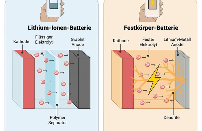
27. 04. 2026 Warum kommt es zu Kurzschlüssen in Festkörper-Batterien?
-
27. 04. 2026 Neuer internationaler Masterstudiengang „Battery Technologies“ startet zum Wintersemester 2026/27
-
27. 04. 2026 Nanofiltration – Wasser wirksam von Glyphosat befreien
-

22. 04. 2026 ZVO-Oberflächentage 2026 erstmals in Karlsruhe: Jetzt anmelden!