
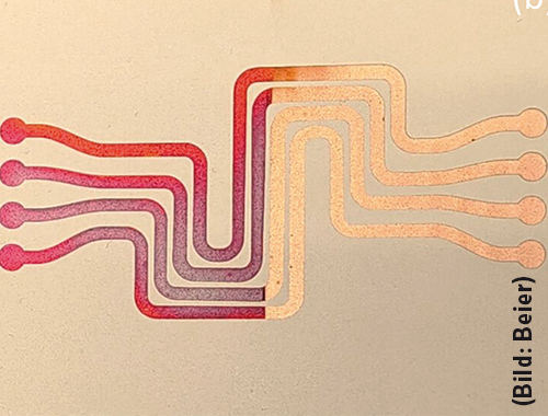



Atmospheric pressure forming gas plasma (95 % N2 / 5 % H2) was investigated for the removal of copper oxide and silver sulfide tarnish layers under ambient conditions. The process enables inline dry treatment without vacuum or chemical etchants, targeting industrial surface restoration. Tarnished layers up to approximately 100 nm were homogenously created and could be successfully reduced by the plasma process. Thickness variations, electrical properties, layer morphology and surface chemistry were analyzed using spectroscopic ellipsometry, 4-point probe measurements, scanning electron microscopy (SEM) and X-ray photoelectron spectroscopy (XPS).
Atmosphärendruck-Plasma zur Entfernung von Oxiden und Sulfiden auf Metalloberflächen
Atmosphärendruck-Plasma (95 % N2 / 5 % H2) wurde zur Entfernung von Kupferoxid- und Silbersulfidbelägen unter Umgebungsbedingungen untersucht. Der Prozess ermöglicht eine Inline-Trockenbehandlung ohne Vakuum oder chemische Ätzmittel und zielt auf die industrielle Oberflächenrestaurierung ab. Beläge bis zu etwa 100 nm wurden homogen erzeugt und konnten erfolgreich durch Plasmabehandlung reduziert werden. Dickenvariationen, elektrische Eigenschaften, Schichtmorphologie und Oberflächenchemie wurden mittels spektroskopischer Ellipsometrie, Vierpunkt-Messungen, Rasterelektronenmikroskopie (REM) und Röntgen-Photoelektronenspektroskopie (XPS) analysiert.
1 Introduction
Copper and silver are widely used in electrical industries and consumer products due to their excellent electrical conductivity, functional reliability and visual appearance. However, exposure to ambient environments leads to the formation of surface oxides and sulfides, such as copper oxides and silver sulfide, which degrade electrical performance, impair solderability, accelerate corrosion, and ultimately reduce manufacturing yield and long-term device reliability [1]. Effective and scalable surface restoration methods are therefore essential for modern high-volume production.
Conventional oxide removal techniques present significant limitations. Wet chemical etching relies on strong acids that pose environmental and safety concerns [2]. Thermal reduction processes require elevated temperatures, catalysts and high energy input [3]. Low-pressure plasma treatments, although effective, demand vacuum systems and complex infrastructure, limiting inline integration and increasing operational costs [4]. Atmospheric plasma treatment offers a promising alternative, enabling rapid, compatible processing under ambient pressure without vacuum equipment [5-7]. Operating at temperatures below 200 °C, this approach is well suited for temperature-sensitive components and high-throughput manufacturing. Under these conditions, copper oxide and silver sulfide are converted to their respective metals, with water vapor or hydrogen sulfide as the primary reaction byproduct, thereby minimizing chemical waste and environmental impact [8-9].
In this study, well-defined copper oxide and silver sulfide layers were prepared to systematically assess the effectiveness of atmospheric-pressure plasma jet (APPJ) treatment using a N2/H2 gas mixture as reducing process gas. The treated surfaces were subsequently analyzed to quantify the degree of reduction and the overall process performance.
2 Experimental Procedures
Due to their industrial significance and vulnerability to surface oxidation, copper and silver were selected for the reduction of oxides and sulfides using atmospheric-pressure plasma. The substrates used in this study included glass slides (75 × 25 mm2), silicon wafers (20 × 10 mm2) and AlMg3 aluminum alloy substrates (90 × 70 mm2) coated with an inorganic plasma chemical oxidation layer (PCO®) [10-11]. Prior to metal deposition, the substrates were subjected to a standardized cleaning procedure to remove surface contaminants. The cleaning process consisted of successive ethanol washes, followed by nitrogen-assisted drying to prevent exposure to moisture and airborne contaminants. Metallic thin films were deposited on these substrate types using a thermal evaporation system in order to obtain continuous and uniform metallic layers with comparable thickness across all samples. On the glass substrates and the silicon wafers, the entire substrate area was either coated with copper or a chromium / silver multilayer. The thin chromium layer (thickness ≈ 10 nm) was applied to improve the adhesion between the glass substrate and the silver layer. On the other hand, conductive paths were created on the PCO®-insulated aluminum substrates by depositing the copper coating through a corresponding shadow mask. This type of material and layer structure offers potential as an aluminum core circuit board (Metal Core Printed Circuit Board – MCPCB). The metal evaporation process for creating copper or chromium / silver films was performed in a chamber (SASKIA Hochvakuum- und Labortechnik) under high-vacuum conditions, with a base pressure of around 3·10–6 mbar, in order to minimize oxidation and impurity incorporation during film growth. High-purity copper, chromium and silver pellets were used as source materials and loaded into the thermal evaporation system. Thin copper or silver films with thicknesses in the range of 200 nm to 300 nm were deposited by controlling the film growth using a quartz crystal microbalance FTM6 system (Edwards). The controlled deposition environment enabled the formation of dense, adherent copper and silver films suitable for the subsequent procedures and plasma treatment.
The formation of copper oxide layers was achieved by thermally annealing copper-coated samples in ambient air using hotplate or oven treatment. Annealing temperatures of 150 °C and 200 °C were employed, with different time periods of 5, 10 and 15 minutes, respectively. After annealing, the samples were allowed to cool naturally to room temperature. Noticeable visual changes were observed following thermal annealing, manifested as color variations on the copper samples. Using the selected annealing times, the oxidation of the applied copper films did not proceed fully throughout the entire film but occurred only partially. Thus, typically after annealing a copper film with an oxidized surface layer was obtained.
The formation of silver sulfide (Ag2S) layers was achieved through an in-situ generation of hydrogen sulfide (H2S) gas, which subsequently reacted with the metallic silver coating. The sulfidation reaction was carried out in a desiccator, thereby promoting hydrogen sulfide generation. To optimize the thickness of the silver sulfide layer, different amounts of sodium sulfide (Na2S) and 85 % orthophosphoric acid (H3PO4) were evaluated: 1 g Na2S with 1 ml H3PO4, 2 g Na2S with 2 ml H3PO4, and 3 g Na2S with 3 ml H3PO4. The thickness of the resulting silver sulfide layer increased with increasing reactant amounts, indicating that the availability of hydrogen sulfide gas directly influences sulfidation kinetics. Based on these observations, the combination of
3 g sodium sulfide and 3 ml orthophosphoric acid was selected as the optimal condition, producing a uniform, adherent, and reproducible silver sulfide layer of around 70 nm thickness after 6 hours of exposure. Shorter interaction times resulted in correspondingly lower layer thicknesses. Conducting the reaction inside a desiccator ensured minimal exposure to atmospheric moisture, enhancing the uniformity and quality of the silver sulfide layer.
The thickness and optical properties of the formed copper oxide and silver sulfide layers were determined by spectroscopic ellipsometry (SE850, Sentech Instruments GmbH). Measurements were performed at incidence angles of 50°, 60°, and 70° over a spectral range of 350 nm to 820 nm. The instrument operates according to the step-scan analyzer principle with a diode array detector, providing high measurement sensitivity. Data evaluation was carried out usingSpectraray II software, enabling the determination of layer thickness, optical constants and surface/interface roughness based on effective medium approximation models. For fitting of the data, a classical oscillator model (for Ag and CuO), a damped oscillator model by Leng [12] (for Ag2S) and an internal data base file layer (for Cu) have been used. Further information on additional analytical methods used, such as 4-point probe measurements to evaluate the sheet resistance, scanning electron microscopy (SEM) and X-ray photoelectron spectroscopy (XPS) are included later.
Plasma surface treatment of metal-coated samples containing copper oxide and silver sulfide on the surface were performed using a commercially available Tigres CAT600 (Fig. 1) atmospheric-pressure plasma jet (APPJ). In this experimental configuration, the plasma nozzle was maintained in a fixed vertical position, while the copper and silver substrates were mounted on a motorized XY-stage. This setup ensured high spatial precision and consistent treatment velocities by translating the samples beneath the stationary plasma discharge. The plasma reduction was performed using forming gas composed of 95 % nitrogen and 5 % hydrogen at an input pressure of 6 bar. The distance from the nozzle to the substrate was maintained at 5 mm to 6 mm for all the experimental runs.
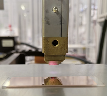
Fig. 1: Experimental setup showing the plasma jet with N2/H2 gas mixture after the treatment procedure of the glass substrates initially containing copper and copper oxide
The translational velocity of the plasma nozzle relative to the sample surface as well as the number of treatments were investigated, in order to control the effective plasma exposure time. The electrical power was also varied within narrow limits.Table 1 gives an overview of the plasma parameter range used for the treatments of the copper oxide and silver sulfide containing samples, respectively.

3 Results
3.1 Plasma reduction of CuO to Cu
Based on ellipsometric investigations it was possible to determine the thickness of the oxidized region on top of the evaporated copper films (Fig. 2). Thus, preliminary thermal oxidation trials revealed a significant influence of the heating method on the formation and uniformity of the resulting copper oxide layer. Specifically, annealing at 200 °C using a convection oven produced a more homogeneous and continuous copper oxide film compared to samples oxidized on a hotplate under similar temperature conditions. The improved uniformity observed for oven-annealed samples is attributed to the isotropic heat distribution and controlled thermal environment provided by the oven. In contrast, hotplate annealing resulted in non-uniform oxidation, likely due to uneven heat transfer at the substrate-heater interface. In all cases, a linear increase of the copper oxide layer thickness with the annealing time was observed. As a result of this investigation, the oven treatment at 200 °C was chosen for further sample preparation, resulting in copper oxide layer thicknesses up to around 100 nm, depending on the annealing time (maximum 15 min).

Fig. 2: Comparison of ellipsometric thickness of layers annealed on a hotplate at 150 °C and 200 °C and in an oven at 200 °C
Reduction of the copper oxide layer occurred locally as the plasma jet traversed the oxidized surface, resulting in a progressive transformation of the oxidized films into metallic copper along the scan path. The post-treatment evaluation was initially performed by visual inspection, which revealed a rapid and pronounced change in surface appearance. Within seconds of plasma exposure, the dark oxide layer was removed, exposing a bright metallic copper surface, indicating effective oxide reduction. Figure 3 shows two examples of the plasma reduction performed on the coated glass slides (top) and the PCO®-insulated aluminum substrates with conductive paths (bottom), respectively.

Fig. 3: Plasma-induced removal of the copper oxide layer and exposure of metallic copper – right side of the sample was plasma treated: copper-on-glass sample (a) and PCO®-insulated aluminum sample with conductive paths (b)
Surface morphology and film thickness evolution were characterized using a combination of ellipsometry and high-resolution scanning electron microscopy (SEM). Spectroscopic ellipsometry was employed as a non-destructive primary technique to evaluate changes in oxide film thickness at each processing stage, including the as-deposited copper films, after thermal oxidation and following atmospheric-pressure plasma treatment. This approach enabled quantitative monitoring of oxide growth and its subsequent reduction, as shown in Figure 4.

Fig. 4: Ellipsometric copper oxide thickness of the copper coatings on glass thermally annealed in an oven at 200 °C with increasing times up to 15 min and after subsequent plasma treatment
Spectroscopic ellipsometry measurements revealed systematic variations in copper oxide film thickness throughout the different processing stages. Initially, the as-deposited copper films with only marginal oxide content after thermal evaporation were analyzed. The ellipsometric parameters of these samples were used as a baseline reference in the layer model for the fitting procedure of the remaining samples and to evaluate the oxide thicknesses after thermal annealing and subsequent plasma treatment. As before, thermal oxidation at 200 °C for 15 min in an oven led to an increase of copper oxide thickness to about 95 nm. Following atmospheric-pressure plasma treatment, the oxide thickness decreased to 6 nm, indicating pronounced oxide reduction. A similar trend was observed for samples with initially thinner oxide layers, produced by shorter annealing times during thermal oxidation. These results demonstrate that ellipsometry provides quantitative insights into oxide growth and plasma-induced changes, confirming its suitability for monitoring thickness evolution throughout the processing sequence.
Changes in the copper oxide content were accompanied by variations in sheet resistance. The sheet resistance on the coated glass samples was measured using a NAGY SD-600 Sheet Resistivity Meter, operating according to the 4-point probe principle. For each sample, the average of three measurements was calculated. Due to the copper oxide formation by oven treatment, an increase in sheet resistance from initially about 80 mΩ (200 nm copper layer) to 100 mΩ was detectable, in the case of copper oxide thicknesses around 100 nm. Following the plasma treatment, the sheet resistance decreased again towards 80 mΩ, improving the electrical properties into the range of the initial copper layers.
After completing the oxide reduction process, the plasma-treated copper samples were analyzed using SEM within 24 hours to limit surface contamination or re-oxidation. In this case, the treated silicon wafer samples were analyzed. Scanning electron microscopy (GeminiSEM 460, Carl Zeiss Microscopy GmbH) was employed to investigate the surface morphology and cross-section of the layers. The acquired images (Fig. 5) provided detailed insights into the microstructural features of the layer.

Fig. 5: SEM images of the coated silicon wafer samples before and after plasma treatment: cross-sectional view (a) and top-view of the untreated reference sample (b), cross-sectional view (c) and top-view after plasma treatment (d)
The SEM cross-sectional images of the as-deposited sample reveal well-defined thickness contrast between the silicon wafer substrate, copper and copper oxide layers. After oven treatment, the copper oxide content that had grown on the copper coating is clearly visible. The plasma treatment led to a marked reduction in contrast between the copper and copper oxide layers, with only a thin surface copper oxide layer visible in the lateral-view SEM images at a 200 nm scale. In the top-view SEM images using the SE detector (secondary electrons), distinct dark and bright gray contrast corresponding to copper and copper oxide layers is evident prior to treatment, whereas post-treatment images show predominantly copper and exhibit nearly identical surface morphology.
3.2 Plasma reduction of Ag2S to Ag
Similar to the copper samples, a pronounced change in the optical appearance was observed after plasma treatment. As the plasma jet traversed the sample surface, a shiny metallic silver surface became visible, indicating the successful reduction of the dark silver sulfide layer to metallic silver (Fig. 6, inset – right side).

Fig. 6: Ellipsometrically determined thickness values of silver coated glass samples containing silver sulfide and after atmospheric pressure plasma-treatment. Inset: Plasma-induced removal of silver sulfide and exposure of metallic silver – right side of the sample was plasma treated
Film thickness and elemental composition were monitored throughout all processing stages using spectroscopic ellipsometry and X-ray photoelectron spectroscopy (XPS). Figure 6 presents the ellipsometry results of the Ag2S layer thickness before and after plasma reduction for three different initial thicknesses.
The evolution of the film thickness, monitored by spectroscopic ellipsometry, reflects the chemical transformation from metallic silver to silver sulfide and its subsequent plasma-mediated reversion. While chemical sulfidation led to a predictable increase in thickness, the atmospheric-pressure plasma treatment effectively removed the sulfur species, resulting in a thickness decrease from about 70 nm to 7 nm. A similar trend was observed for the thinner silver sulfide layers. These data indicate that the atmospheric plasma process achieves an almost complete reduction of the sulfide layer from the treated samples.
XPS analysis performed with an Axis Ultra DLD device (Kratos Analytical Ltd.) complemented the ellipsometry measurements by providing surface-sensitive chemical information, enabling detailed assessment of the transition from sulfide formation to plasma-assisted reduction. The combination of both techniques allowed a comprehensive evaluation of thickness variation and chemical state changes during the treatment sequence. Following completion of the silver sulfide reduction process, the plasma-treated silver samples were analyzed within 24 hours to minimize surface contamination or re-sulfidation effects.Figure 7 shows, as an example, the elemental concentrations of silver, sulfur, oxygen and carbon in the surface region of an as-deposited silver coating, after silver sulfide formation and after subsequent plasma treatment.

Fig. 7: Elemental concentrations by XPS of the silver coated silicon wafer samples for the as-deposited silver layer, chemically sulfided silver sulfide layer and plasma-treated layer
XPS analysis revealed a clear reduction of the silver sulfide layer formed after chemical treatment following atmospheric plasma exposure. After sulfidation, the surface exhibited a reduced silver content (27.2 at.%) and an elevated sulfur concentration (9.1 at.%) compared to the silver layer after deposition. The accompanying increase of carbon content is most probably attributed to carbon adsorptions from the environment and slight time differences between storage and introducing the samples into the XPS. Oxygen remained at a comparable level for both samples.
After plasma treatment, the sulfur concentration decreased significantly to 0.3 at.%, while the silver atomic percentage increased to 51.9 at.%, approaching the surface composition of the metallic silver layer. A pronounced decrease in carbon content was also observed, which is most likely related to the removal of surface adsorbates during plasma exposure. It should be noted that XPS examines only the near-surface region with an information depth of approximately 10 nm. Consequently, species adsorbed from the atmosphere or surface contaminations may influence the detected elemental composition, particularly for carbon and oxygen. Therefore, the measured elemental concentrations should be interpreted with respect to the surface sensitivity of the method. Furthermore, minor variations may arise from differences in the analyzed samples and measurement locations.
In order to obtain additional information on the binding states of silver, the XPS detail spectrum was evaluated. Both the peak positions (binding energy of Ag 3d and kinetic energy of Auger electrons) and the characteristic peak shape indicate that the layer surface consists of metallic silver for the samples with an evaporated silver layer and after plasma reduction of silver sulfide to silver as well. These results confirm the efficient plasma-induced reduction of the silver sulfide layer to metallic silver and the effective removal of sulfur species from the surface. Furthermore, the plasma treatment with forming gas in ambient air atmosphere slightly changes the oxygen content in comparison to the evaporated metallic silver layer, which can be caused e.g. by oxidation of the remaining carbon directly at the layer surface. However, the evaluated carbon detail spectra do not show clear results here. To determine the chemical bonds of the measured oxygen content for all three cases, further investigations have to be carried out in the future.
4 Conclusion and Outlook
Experimental results demonstrate that forming-gas-based atmospheric-pressure plasma processing effectively removes copper oxide layers with thicknesses in the investigated range up to hundred nanometers. The treatment restores metallic copper surfaces, improving electrical conductivity and surface reliability. A comparable reduction behavior is observed for silver sulfide. The approach is potentially extendable to other technologically relevant metals such as tin, where oxide removal is critical for reliable interconnections.
The need for reduction of copper, silver and tin surfaces arises primarily in semiconductor packaging, printed circuit board (PCB) assembly, power electronics, lead-frame manufacturing, wire bonding and soldering and advanced electronic interconnected technologies. In these applications, surface oxides and sulfides inhibit solder wetting, increase contact resistance, reduce bond strength and accelerate corrosion, ultimately lowering manufacturing yield and long-term device performance.
By adjusting plasma power, scan velocity and number of treatments, the atmospheric plasma process enables controlled and efficient removal of oxide and sulfur layers under ambient conditions. Its compatibility with continuous production systems makes it highly suitable for high-volume industrial manufacturing. Moreover, the reduced reliance on chemical cleaning agents promotes safer, more environmentally sustainable processing. Utilizing forming-gas-based atmospheric-pressure plasma processing therefore presents an effective, scalable solution for advanced electronic assembly and packaging technologies, combining improved surface functionality with environmentally responsible manufacturing.
Acknowledgements
The authors would like to thank Dr. Martina Schweder, Thomas Seemann and Sven Hartmann for their contributions to copper and chromium / silver deposition, cross-section preparation, SEM and XPS analyses.
References
[1] IBE Electronics. Dealing with PCB Surface Oxidation – Understanding, Prevention, and Solutions; https://www.pcbaaa.com/pcb-surface-oxidation/, accessed on 23.02.2026
[2] K. L. Chavez, D. W. Hess: A novel method of etching copper oxide using acetic acid; Journal of The Electrochemical Society (2001), 148, 11, pp. G640 - G643
[3] J. J. Navarro, M. Das, S. Tosoni, F. Landwehr, M. Heyde, G. Pacchioni, F. Glorius, B. Roldan Cuenya: Promoted thermal reduction of copper oxide surfaces by N-heterocyclic carbenes; The Journal of Physical Chemistry C (2022), 126, 41, pp. 17528 – 17535
[4] C. X. Yi, S. K. Wang, X. B. Xu, Y. F. Tian, M. D. Bao: Study on plasma cleaning of surface contaminants on pure copper; Materials Research Express (2023), 10, 1, 016506
[5] M. E. Sener, S. Sathasivam, R. Palgrave, R. Q. Cabrera, D. J. Caruana: Patterning of metal oxide thin films using a H2/He atmospheric pressure plasma jet; Green Chemistry (2020), 22, 4, pp. 1406 - 1413
[6] Plasmatreat GmbH:Inline Oxide Reduction; https://www.plasmatreat.com/en/products-and-services/openair-plasmar-systems/inline-oxide-reduction, accessed on 23.02.2026
[7] D. Korzec, I. Doelfs, M. Trabold: Oxidation beim Plasmareinigen von Metall; Galvanotechnik (2025), 4, pp. 504 – 506
[8] D. Pappas, A. Sy, R. Robinson, R. Burke: Metal oxide removal using atmospheric pressure plasma technology for electronic applications; IMAPS 2022 - 55th International Symposium on Microelectronics, October 3-6, 2022, Boston, MA USA
[9] O. Schalm, A. Patelli, P. Storne, A. Crabbé, S. Voltolina, V. Feyer, H. Terryn: Tarnished silver–copper surfaces reduction using remote helium plasma at atmospheric pressure studied by means of high-resolution synchrotron x-ray photoelectron microscopy; Corrosion Science (2021), 178, 109074
[10] J. Schmidt, C. Schrader, M. Tzschach: Die plasmachemische Oxidation von Leichtmetallen für optische und medizinische Anwendungen; Jahrbuch Oberflächentechnik (2011), 67, pp. 192 – 202
[11] INNOVENT e.V.: Plasmachemische Oxidation - PCO®; https://www.coating-innovent.com/verfahren/plasmachemische-oxidation-pcor, accessed on 23.02.2026
[12] J. Leng, J. Opsal, H. Chu, M. Senko, D. E. Aspnes: Analytic representations of the dielectric functions of materials for device and structural modelling; Thin Solid Films (1998), 313 – 314, pp. 132 – 136