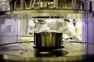
Pulling crystals for semiconductor technology
The GaAs crystals are sawn into wafers before being subsequently polished in a chemical-physical process / Bildquelle: Freiberger Compound Materials GmbH
Crystalline semiconductor components form the core of many modern communication technologies such as computers and mobile phones. They are produced during a multi-day pulling process that uses considerable energy. The BINE-Projektinfo brochure “Efficient production of monocrystalline semiconductors” (01/2015) presents a new method for producing gallium arsenide crystals. Instead of growing individual crystals as was previously the case, nine crystals are now grown in parallel from the melt. This reduces the specific energy consumption for the production by two thirds.
In addition to silicon, which still dominates semiconductor technology, gallium arsenide has also established itself as a substrate material for high-purity single crystals. With these crystals the atoms are arranged in an almost perfect lattice, whereby only every millionth atom is a foreign element. The crystals are pulled from hot melt, which has a temperature of up to 1300 °C, during a process that takes several days. With the new method, the developers have succeeded in increasing both the solidification rate and yield. The challenge with parallel growth is to supply the heat and arrange the nine crystals in such a manner that the structure and purity of the final product are not impaired.
The new method has been developed by the Freiberger Compound Materials (FCM) company. Dr Berndt Weinert, R&D Manager at FCM: “The method has proved itself in practice and the production has almost completely moved over to using it. An estimated 4000 MWh were saved in 2014.” The company has since then converted its entire production to the new method.
Aktuelle Onlineartikel
-
11. 05. 2026 Fluorfreie Trockenbeschichtung für leistungsfähige Batterien
-
11. 05. 2026 Laserdirektplattieren senkt Taktzeit und Kosten für dicke Metallbeschichtungen
-
27. 04. 2026 Warum kommt es zu Kurzschlüssen in Festkörper-Batterien?
-
27. 04. 2026 Neuer internationaler Masterstudiengang „Battery Technologies“ startet zum Wintersemester 2026/27
-
27. 04. 2026 Nanofiltration – Wasser wirksam von Glyphosat befreien
-

22. 04. 2026 ZVO-Oberflächentage 2026 erstmals in Karlsruhe: Jetzt anmelden!